
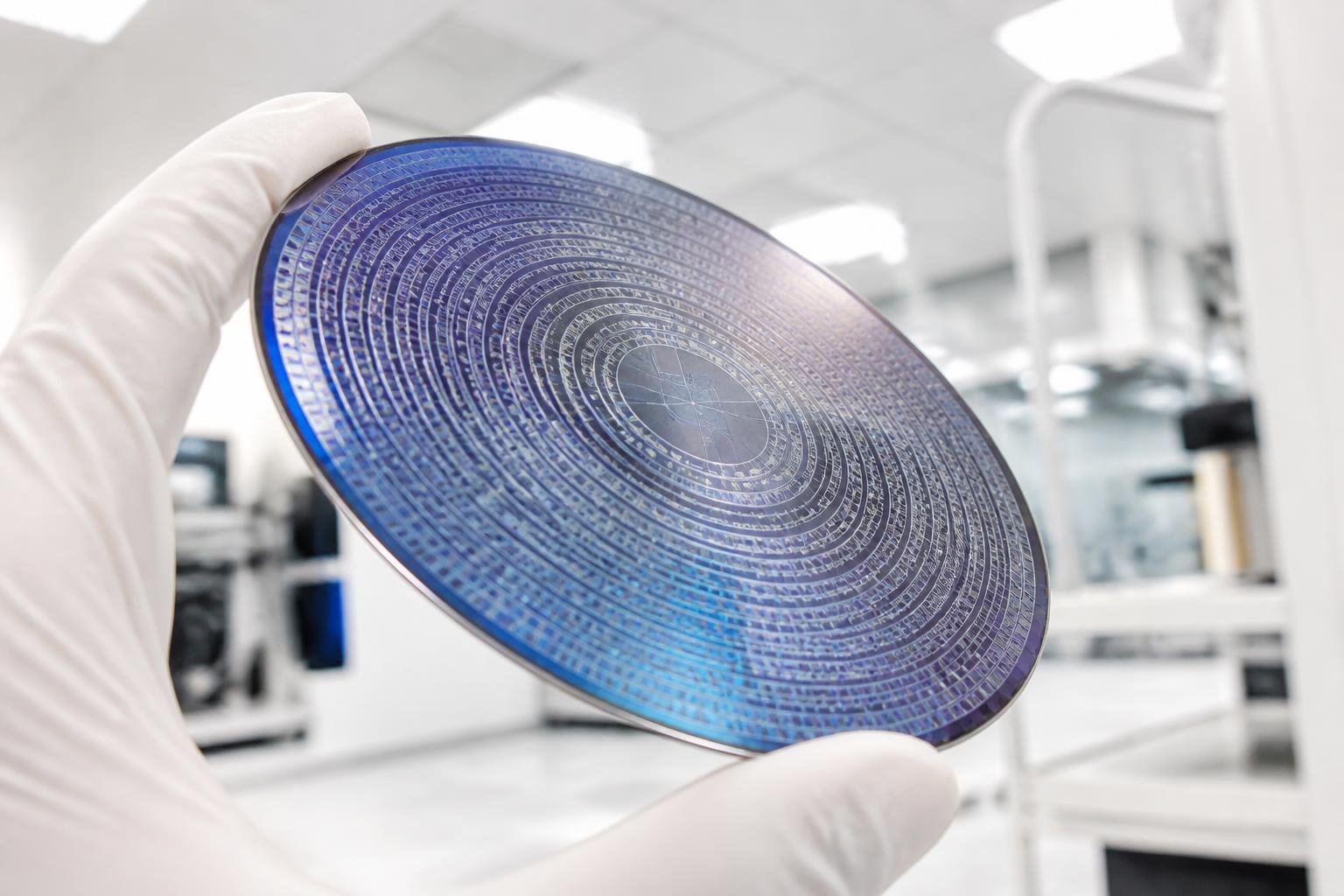
The semiconductor industry has long lived under the shadow of a looming question: is Moore's Law approaching its limit? IBM believes it now has an answer. According to MIT Technology Review, the company has presented a prototype chip in which approximately 100 billion transistors are densely packed into an area no larger than a fingernail — double the density of IBM's previous leading-edge technology, which launched in 2021.
What Makes This Possible?
IBM's new design is not merely an incremental improvement. The company is now working with transistor geometries below one nanometer, a threshold that represents a significant technological leap. Shorter distances between transistors mean signals can travel faster and chips consume less power per operation — an increasingly critical criterion at a time when data centers and artificial intelligence are placing enormous pressure on global energy consumption.
The prototype itself is a roadmap rather than a finished product, but according to MIT Technology Review it points toward a possible future in which the semiconductor industry can continue scaling performance and efficiency for at least another decade.
IBM believes its new chip technology could extend Moore's Law by a decade — and the industry is watching closely.
An Industry Race in Full Swing
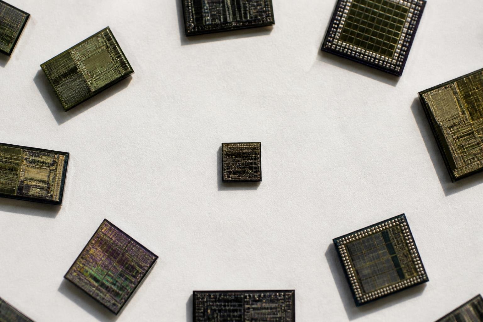
IBM is far from alone in the race to build the smallest transistors. Research sources indicate that the three dominant players in semiconductor manufacturing — Intel, TSMC, and Samsung — are all deep into the development of sub-2nm technology.
Intel has entered what the company itself calls the "Angstrom Era." Its Intel 18A process (equivalent to the 1.8nm class) is now in high-volume production after launching in late 2025. The technology uses so-called RibbonFET gate-all-around (GAA) transistors and a new backside power delivery network called PowerVia. Compared to the previous Intel 3 node, 18A is said to deliver 15 percent better energy efficiency and 30 percent higher density. Intel is already working on a 14A process planned for high-volume production in 2029, and according to research sources the company has begun early development work on even more advanced 10A and 7A nodes.
TSMC, the world's largest contract chip manufacturer, began volume production of its 2nm process (N2) in the fourth quarter of 2025. According to available industry figures, the company controlled approximately 72 percent of revenue among the top ten fabrication services in 2025. TSMC is already developing A16 and A14 technology, with the latter slated for volume production around 2029.
Samsung Foundry began mass production of its first 2nm process (SF2) in 2025, but has encountered yield challenges. Early figures from 2026 suggested yields were running in the 50–60 percent range for the 2nm node. The company has an ambitious target of mass-producing 1.4nm technology by 2027, though industry observers are skeptical about whether that timeline is realistic.
Moore's Law: Not Dead, but Transformed
The traditional rule of thumb that transistor density doubles roughly every two years — Moore's Law — has long shown signs of flattening. Industry experts point out that going forward, simply shrinking transistors further will not be the sole driver of progress. Techniques such as three-dimensional layer stacking and advanced chip packaging will play an increasingly important role. These methods make it possible to boost performance and reduce energy consumption without the costs of continued physical scaling becoming prohibitive.
Extreme ultraviolet (EUV) lithography is considered a necessity for manufacturing chips below 2nm, and is estimated to account for more than half of the semiconductor industry's lithography needs in the years ahead.
What Does This Mean in Practice?
For end users and industry alike, advances like IBM's prototype open the door to faster processors, more energy-efficient AI accelerators, and more compact devices. It is important to note, however, that IBM has presented a prototype — the road from laboratory to mass production is long and costly, and there is no guarantee that design specifications will survive the transition to production at scale.
Nevertheless, IBM's announcement sends a clear signal to the industry: the race to build the smallest and densest chips is far from over.
Sources: MIT Technology Review, industry research analysis on Intel, TSMC, and Samsung Foundry.